The TB6612FNG is a dual-channel DC motor driver module built around the Toshiba TB6612FNG LD MOS H-bridge IC that controls the speed and direction of two DC motors or one bipolar stepper motor simultaneously. By combining two full H-bridges with very low RDSon MOSFET output transistors, a standby power-save mode, and four selectable operating modes per channel, it delivers efficient and precise motor control with significantly lower power dissipation than older Darlington-based drivers such as the L298N.
Pinout
The bare TB6612FNG IC is a 24-pin SSOP package and is not breadboard-compatible. It is used on a breakout module in virtually all maker applications. Most breakout modules expose all control and power pins through two rows of through-hole headers on opposite edges of the board, with motor output screw terminals or pads on the sides.
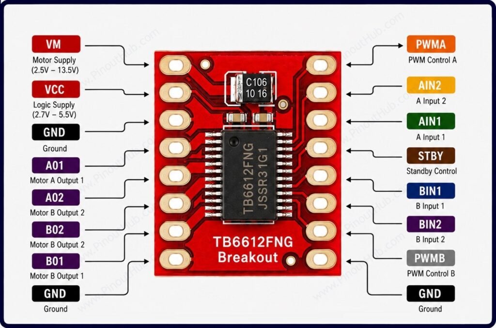
Breakout module pinout
| Pin | Name | Type | Description |
|---|---|---|---|
| 1 | VMOT | Power | Motor supply voltage — 4.5V to 13.5V DC |
| 2 | VCC | Power | Logic supply voltage — 2.7V to 5.5V; powers the IC control logic |
| 3 | GND | Power | Ground — common for motor supply and logic |
| 4 | STBY | Input | Standby — pull HIGH for normal operation; pull LOW to disable both channels and enter standby mode |
| 5 | AIN1 | Input | Channel A direction control input 1 |
| 6 | AIN2 | Input | Channel A direction control input 2 |
| 7 | PWMA | Input | Channel A PWM speed control — connect to microcontroller PWM pin; duty cycle controls Motor A speed |
| 8 | AO1 | Output | Channel A motor output terminal 1 |
| 9 | AO2 | Output | Channel A motor output terminal 2 |
| 10 | BIN1 | Input | Channel B direction control input 1 |
| 11 | BIN2 | Input | Channel B direction control input 2 |
| 12 | PWMB | Input | Channel B PWM speed control — connect to microcontroller PWM pin; duty cycle controls Motor B speed |
| 13 | BO1 | Output | Channel B motor output terminal 1 |
| 14 | BO2 | Output | Channel B motor output terminal 2 |
STBY pin: The STBY pin must be pulled HIGH for the driver to operate. Most breakout modules include a pull-down resistor on STBY — meaning it must be actively driven HIGH by a microcontroller GPIO pin or tied to VCC via a jumper. Leaving it floating or LOW disables both channels regardless of the IN and PWM pin states.
PWMA / PWMB: Driving the PWM pins with a digital HIGH enables the channel at full speed. Driving with a PWM signal from the microcontroller controls motor speed proportionally to duty cycle. The TB6612FNG accepts PWM frequencies up to 100kHz — well above the audible range — allowing silent speed control without motor whine.
Motor Control Truth Table
Channel A (AIN1 / AIN2 / PWMA / STBY)
| AIN1 | AIN2 | PWMA | STBY | Output |
|---|---|---|---|---|
| HIGH | LOW | HIGH | HIGH | Clockwise (CW) |
| LOW | HIGH | HIGH | HIGH | Counter-clockwise (CCW) |
| LOW | LOW | HIGH | HIGH | Stop (coast) |
| HIGH | HIGH | HIGH | HIGH | Short brake |
| X | X | LOW | HIGH | Stop (coast) |
| X | X | X | LOW | Standby |
Channel B (BIN1 / BIN2 / PWMB / STBY) — same logic as Channel A with BIN1, BIN2, and PWMB.
Short brake vs Stop: In short brake mode (both IN pins HIGH), both low-side transistors of the H-bridge are turned ON simultaneously, creating a short circuit across the motor terminals and causing rapid deceleration through regenerative braking. In stop mode (both IN pins LOW), all transistors are OFF and the motor coasts to a stop freely.
Module Construction
TB6612FNG IC A 24-pin SSOP package containing two full LD MOS H-bridge circuits, internal freewheeling diodes, standby control logic, thermal shutdown circuit, and under-voltage lockout. All motor control, switching, and protection functions are integrated within this single IC.
Decoupling Capacitors The datasheet recommends noise-absorption capacitors C1–C4 placed as close as possible to the IC on both the VM and VCC supply pins. Most breakout modules include 100nF ceramic capacitors on both rails plus a larger bulk capacitor on VMOT to absorb motor switching transients.
Internal Freewheeling Diodes Built into the LD MOS transistor structure of each H-bridge output. Absorb back-EMF voltage spikes from motor windings when they are de-energized, eliminating the need for external freewheeling diodes.
Logic Level Header A pin header exposing AIN1, AIN2, PWMA, BIN1, BIN2, PWMB, STBY, VCC, and GND for direct connection to microcontroller GPIO and PWM pins.
Motor Output Pads / Terminals AO1, AO2, BO1, and BO2 are exposed as through-hole pads or screw terminals on the breakout board for connecting motor leads.
Specifications
| Parameter | Value |
|---|---|
| Supply | |
| Motor Supply Voltage (VM) | 4.5V – 13.5V DC |
| Logic Supply Voltage (VCC) | 2.7V – 5.5V |
| Standby Current | ~0µA |
| Output | |
| Continuous Output Current | 1.2A per channel |
| Peak Output Current | 3.2A per channel |
| Output RDSon (upper + lower) | 0.5Ω typical at VM ≥ 5V |
| PWM Frequency | Up to 100kHz |
| Operating Modes | |
| Channel Modes | CW / CCW / Short Brake / Stop |
| Standby Mode | Yes (STBY pin) |
| Protection | |
| Internal Freewheeling Diodes | Yes |
| Thermal Shutdown | Yes |
| Under-Voltage Lockout | Yes |
| Control | |
| Logic Input Levels | 2.7V – 5.5V |
| Number of H-Bridges | 2 |
| Motor Channels | 2 DC motors / 1 bipolar stepper |
| General | |
| Operating Temperature | −20°C to +85°C |
| IC Package | SSOP-24 |
| RoHS | Compliant |
Helpful resources
- Download the datasheet: here
- TB6612FNG with Arduino
- TB6612FNG with ESP32
- TB6612FNG with Raspberry Pi Pico