The INA219 is a zero-drift bidirectional current and power monitor IC manufactured by Texas Instruments that simultaneously measures shunt voltage, bus voltage, current, and power and reports all four values digitally over I²C. By combining a precision amplifier, a 12-bit ADC, a programmable calibration register, and an internal power multiplier in a single chip, it delivers direct readouts in milliamps and milliwatts without requiring any external signal conditioning.
Pinout
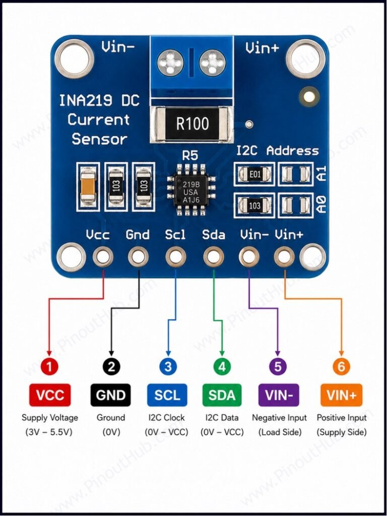
| Pin | Name | Type | Description |
|---|---|---|---|
| 1 | VCC | Power | Supply input — 3V to 5.5V; powers the INA219 IC and onboard logic |
| 2 | GND | Power | Ground |
| 3 | SCL | Input | I²C clock line — connect to microcontroller SCL; 10kΩ pull-up included on most modules |
| 4 | SDA | I/O | I²C data line — connect to microcontroller SDA; 10kΩ pull-up included on most modules |
| 5 | Vin- | Input | I²C address bit 0 — solder jumper on module; changes I²C base address when bridged |
| 6 | Vin+ | Input | I²C address bit 1 — solder jumper on module; changes I²C base address when bridged |
High-current measurement side (2 terminals)
| Terminal | Name | Description |
|---|---|---|
| + | VIN+ | Positive current input — connect to the supply side of the circuit under measurement |
| − | VIN− | Negative current output — connect to the load side; bus voltage is measured at this pin |
I²C addressing: The A0 and A1 pins allow up to four I²C addresses per module by bridging solder jumpers on the board. The full 16-address range of the IC is accessed by connecting A0 and A1 to GND or VS in different combinations. Default address with both pins open (GND) is 0x40.
| A1 | A0 | I²C Address |
|---|---|---|
| GND | GND | 0x40 (default) |
| GND | VCC | 0x41 |
| VCC | GND | 0x44 |
| VCC | VCC | 0x45 |
INA219 module construction
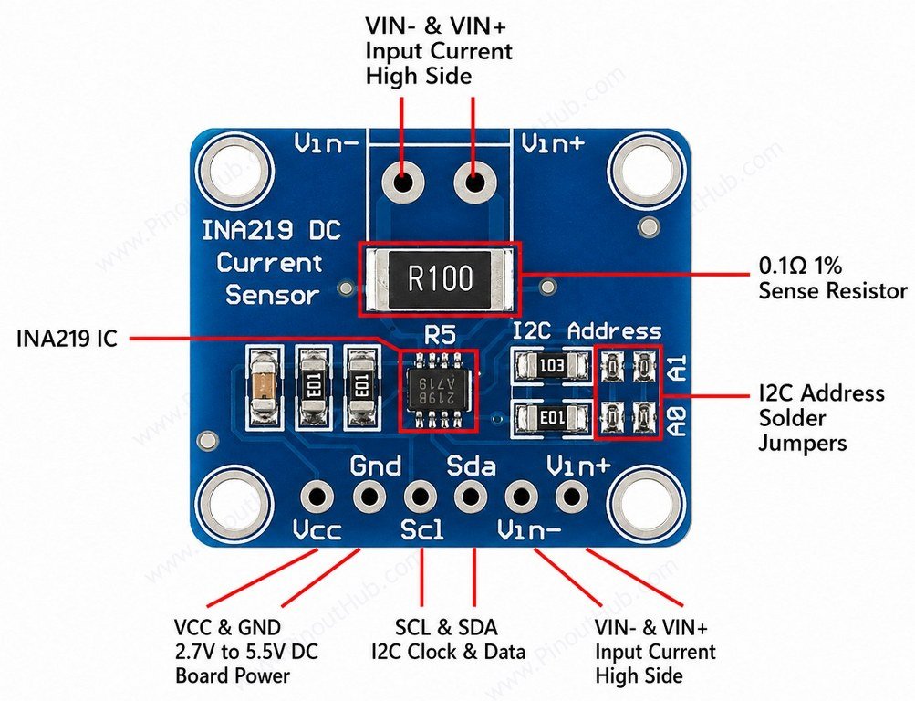
INA219 Sensor IC A SOT23-8 or SOIC-8 package containing the precision differential amplifier, two 12-bit ADC channels, programmable gain amplifier, calibration register, internal power multiplier, and I²C interface logic. All current, voltage, and power calculations are performed onboard — the host only reads the finished register values.
0.1Ω Shunt Resistor A 1% precision, 2W rated resistor pre-soldered on the high-current path between VIN+ and VIN−. This is the element across which the INA219 measures the voltage drop to determine current. It can be desoldered and replaced with a different value to change the sensing range — the calibration register must be updated accordingly.
I²C Pull-up Resistors Onboard pull-up resistors on the SDA and SCL lines. On modules that do not include them, external 4.7kΩ pull-ups between each line and VCC are required for reliable I²C communication.
A0 / A1 Address Solder Jumpers Two solder pads on the board that, when bridged, pull the A0 or A1 address pins to VCC. Leaving them open connects them to GND. Combining these two jumpers gives four selectable I²C addresses per board without requiring any external wiring.
Decoupling Capacitor A 0.1µF ceramic capacitor between VS and GND, placed close to the IC, filters high-frequency supply noise. The datasheet recommends a value between 0.1µF and 1.0µF for stable operation.
Screw Terminals / High-Current Pads The VIN+ and VIN− connection points on the high-current side of the board. Most modules provide either screw terminals for wire connections or large through-hole pads for soldering heavier gauge wiring.
Specifications
| Parameter | Value |
|---|---|
| Supply | |
| Supply Voltage (VS) | 3V – 5.5V |
| Supply Current | 1mA maximum |
| Measurement | |
| Bus Voltage Range | 0V – 26V |
| Shunt Voltage Range | ±320mV (gain = 1) |
| ADC Resolution | 12-bit |
| Current Range (0.1Ω shunt) | ±3.2A |
| Current Resolution (0.1Ω shunt) | 0.8mA |
| Accuracy (INA219A) | ±1% over temperature |
| Accuracy (INA219B) | ±0.5% over temperature |
| Sample Averaging | 1 / 2 / 4 / 8 / 16 / 32 / 64 / 128 samples |
| Interface | |
| Communication | I²C / SMBus |
| I²C Speed | Up to 400kHz |
| I²C Addresses | 16 programmable (0x40 – 0x4F) |
| Default I²C Address | 0x40 |
| General | |
| Operating Temperature | −40°C to +85°C |
| Package | SOT23-8 / SOIC-8 |
| RoHS | Compliant |
Helpful resources
- Download the datasheet: here
- INA219 with Arduino
- INA219 with ESP32
- INA219 with Raspberry Pi