The DRV8833 is a dual H-bridge motor driver module built around the Texas Instruments DRV8833 IC that drives two DC brush motors or one bipolar stepper motor simultaneously using N-channel power MOSFETs with integrated current regulation.
By combining two full H-bridges, onboard winding current limiting, a fault output pin, and a low-power sleep mode in a single chip, it delivers efficient and protected bidirectional motor control in an ultra-compact footprint suitable for battery-powered applications.
Pinout
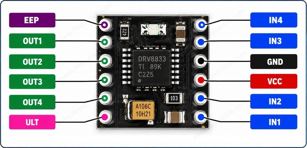
| Pin | Name | Type | Description |
|---|---|---|---|
| 1 | VCC | Power | Motor supply voltage — 2.7V to 10.8V DC; connect to motor power supply |
| 2 | GND | Power | Ground — common for motor supply and logic |
| 3 | IN1 | Input | Bridge A direction control input 1 — connect to microcontroller GPIO or PWM pin |
| 4 | IN2 | Input | Bridge A direction control input 2 — connect to microcontroller GPIO or PWM pin |
| 5 | IN3 | Input | Bridge B direction control input 1 — connect to microcontroller GPIO or PWM pin |
| 6 | IN4 | Input | Bridge B direction control input 2 — connect to microcontroller GPIO or PWM pin |
| 7 | OUT1 | Output | Bridge A motor output terminal 1 — connect to one terminal of Motor A |
| 8 | OUT2 | Output | Bridge A motor output terminal 2 — connect to other terminal of Motor A |
| 9 | OUT3 | Output | Bridge B motor output terminal 1 — connect to one terminal of Motor B |
| 10 | OUT4 | Output | Bridge B motor output terminal 2 — connect to other terminal of Motor B |
| 11 | EEP | Input | Sleep pin — HIGH enables the device; LOW enters low-power sleep mode and resets all internal logic |
| 12 | FLT | Output | Fault output — open-drain, active LOW; goes LOW when overcurrent or overtemperature fault is detected |
EEP (Sleep) pin: Must be pulled HIGH for normal operation. Most breakout modules include an onboard pull-up resistor so EEP defaults HIGH when left unconnected. Pulling EEP LOW disables all outputs and resets internal logic, reducing supply current to approximately 500nA. The IC requires up to 1ms after EEP returns HIGH before outputs are fully operational.
FLT (Fault) pin: Open-drain output requiring a pull-up resistor to logic VCC — most breakout modules include a 10kΩ pull-up. Goes LOW when the IC detects an overcurrent or overtemperature condition. Connect to a GPIO interrupt-capable pin on the microcontroller to detect and handle fault conditions in firmware.
Module construction
The DRV8833 motor driver module consists of the following components:
DRV8833 IC A 16-pin surface-mount package (WQFN, HTSSOP, or TSSOP depending on module variant) with a PowerPAD thermal pad on the underside that conducts heat to the PCB ground plane. Contains two complete N-channel MOSFET H-bridges, integrated charge pump for high-side gate drive, winding current regulation circuitry, nFAULT logic, nSLEEP control, thermal shutdown, overcurrent protection, and under-voltage lockout.
ISEN Sense Resistors One resistor per H-bridge channel connected between the ISEN pin and GND. Sets the peak current limit in conjunction with the VREF voltage. On modules where current regulation is not configured, these resistors connect ISEN directly to GND, disabling active current regulation and relying solely on the IC’s internal overcurrent shutdown.
10µF Low-ESR Ceramic Decoupling Capacitor Placed between VM and GND as close to the IC as possible, as specified in the datasheet. Low-ESR ceramic construction is required — electrolytic capacitors have too much ESR to adequately suppress the high-frequency switching transients from the N-channel H-bridge gate charge pump. A second capacitor between VM and VCP (charge pump supply) is also required per the datasheet.
nFAULT Pull-up Resistor A 10kΩ resistor between nFAULT and logic VCC. Required because nFAULT is an open-drain output — without a pull-up, the pin floats HIGH and cannot produce a valid logic HIGH when no fault is present.
nSLEEP Pull-up Resistor A resistor between nSLEEP and VM on most modules, keeping the driver active by default. The datasheet recommends a pull-up resistor (rather than a direct tie) when VM exceeds 6.5V, since the nSLEEP pin has an internal 6.5V Zener clamp — currents greater than 250µA into the pin can damage the input structure.
Control and Power Headers Through-hole pin headers exposing VM, GND, AIN1, AIN2, BIN1, BIN2, nSLEEP, nFAULT, AOUT1, AOUT2, BOUT1, and BOUT2 for direct connection to microcontroller GPIO, PWM, and motor leads.
Specifications
| Parameter | Value |
|---|---|
| Supply | |
| Motor Supply Voltage (VM) | 2.7V – 10.8V DC |
| Logic Input Voltage | 1.8V – VM |
| Sleep Current (nSLEEP = LOW) | 500nA typical |
| Quiescent Current (no load) | 1.5mA typical |
| Output | |
| Continuous Output Current (RMS) | 1.5A per H-bridge (VM = 5V, 25°C) |
| Peak Output Current | 2A per H-bridge |
| RDSon (HS + LS) | 360mΩ typical |
| Current Regulation | |
| Current Limit Formula | ILIMIT = VREF ÷ (5 × RSEN) |
| Decay Mode | Slow decay (default) |
| Protection | |
| Overcurrent Protection | Yes |
| Thermal Shutdown | Yes (~150°C junction) |
| Under-Voltage Lockout | Yes |
| Short Circuit Protection | Yes |
| nFAULT Output | Active LOW, open-drain |
| Control | |
| PWM Speed Control | Yes |
| nSLEEP | Active LOW |
| Motor Channels | 2 DC motors / 1 bipolar stepper |
| General | |
| Operating Temperature | −40°C to +85°C |
| IC Package | 16-pin WQFN / HTSSOP / TSSOP |
| RoHS | Compliant |
Helpful resources
- Download the datasheet: here
- DRV8833 with Arduino
- DRV8833 with ESP32
- DRV8833 with Raspberry Pi