The ACS712 is a fully integrated Hall effect based linear current sensor IC that measures both AC and DC current and outputs an analog voltage directly proportional to the sensed current.
By routing the current under measurement through a low-resistance internal conductor and sensing the resulting magnetic field with an integrated Hall element, it provides galvanic isolation between the high-current path and the signal output — the measuring circuit never makes electrical contact with the circuit being measured.
Pinout
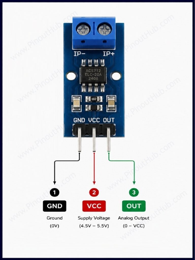
| Pin | Name | Type | Description |
|---|---|---|---|
| 1 | VCC | Power | 5V supply input for the signal circuit |
| 2 | GND | Power | Ground for the signal circuit |
| 3 | OUT | Output | Analog voltage output — 2.5V at zero current; rises above 2.5V for positive current; falls below for negative current |
| 4 | IP+ | Current Input | High-current input terminal — connect to the current source |
| 5 | IP− | Current Output | High-current output terminal — connect to the load |
High-current side: The IP+ and IP− terminals carry the current under measurement. They are rated for the maximum current of the selected variant (5A, 20A, or 30A). These terminals must be wired with wire gauge appropriate for the expected current — do not use standard jumper wires for high-current applications.
Signal side: VCC, GND, and OUT operate at low voltage and connect directly to the microcontroller. OUT connects to any ADC input. A 0.1µF bypass capacitor between VCC and GND, placed close to the module, is recommended to suppress supply noise on the output.
Isolation: The 2.4kVRMS galvanic isolation between the IP+/IP− side and the VCC/GND/OUT side means the high-current circuit and the microcontroller circuit are electrically isolated. However, the IP+/IP− terminals on most breakout boards are rated for lower voltages than the IC maximum — always check the breakout board’s own voltage rating before connecting to mains or high-voltage circuits.
ACS712 module construction
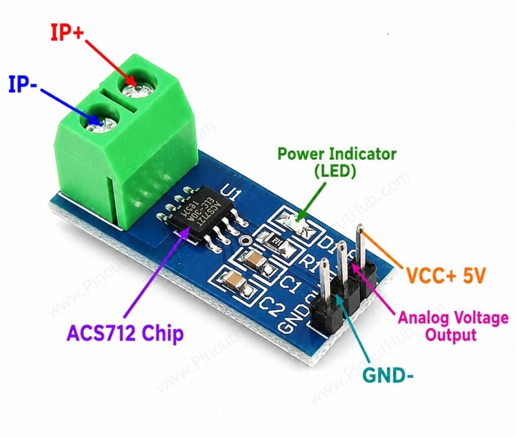
ACS712 Sensor IC An SOIC-8 package containing the internal copper conductor, Hall effect sensing element, differential amplifier, low-pass filter, and output buffer. The 1.2mΩ internal conductor resistance minimises power dissipation and voltage drop in the high-current path.
High-Current Terminals (IP+ / IP−) Two screw terminals or through-hole pads on one edge of the breakout board. These carry the current under measurement and are physically separated from the signal side of the board. Wire gauge must be appropriate for the current variant in use.
Signal Header (VCC, GND, OUT) A 3-pin header on the opposite edge of the board from the current terminals, connecting the signal circuit to the microcontroller. Keeps signal wiring physically and electrically away from the high-current path.
0.1µF Bypass Capacitor Connected between VCC and GND on the signal side to suppress high-frequency noise on the supply rail. Prevents supply transients from appearing as false current readings on the OUT pin.
1nF FILTER Capacitor Connected between the FILTER pin and GND on most breakout boards. Sets the default output bandwidth to approximately 80kHz. Can be replaced with a larger value to reduce bandwidth and noise in low-frequency applications.
Specifications
| Parameter | Value |
|---|---|
| Supply | |
| Supply Voltage (VCC) | 5V only |
| Supply Current | 10mA typical |
| Output | |
| Output Type | Analog voltage, ratiometric |
| Output at Zero Current | 2.5V |
| Sensitivity (±5A) | 185 mV/A |
| Sensitivity (±20A) | 100 mV/A |
| Sensitivity (±30A) | 66 mV/A |
| Output Rise Time | 5µs |
| Bandwidth | 80kHz |
| Total Output Error | 1.5% at 25°C |
| Isolation | |
| Galvanic Isolation | 2.4kVRMS minimum |
| Internal Conductor Resistance | 1.2mΩ |
| General | |
| Operating Temperature | −40°C to +85°C |
| Package | SOIC-8 |
| RoHS | Compliant |
Helpful resources
- Download the datasheet: here
- ACS712 with Arduino
- ACS712 with ESP32